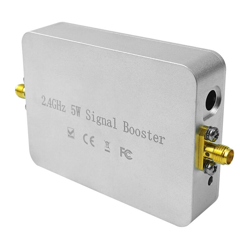
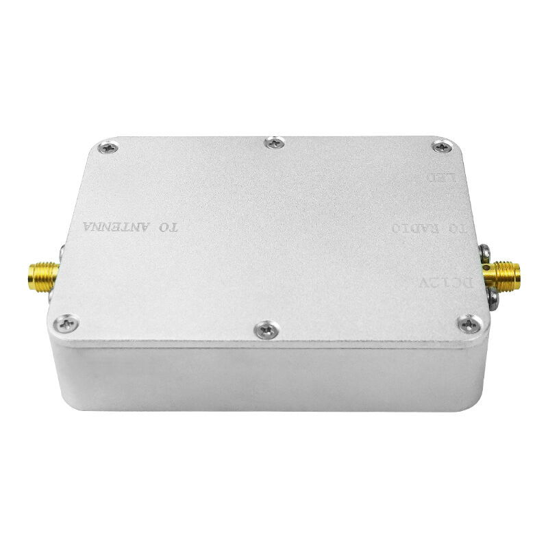
WIFI 5g 5.2ghz 5.8ghz 10W HD signl booster dual band power amplifier for drone signal extender
TXSZS520010 is special designed for high-definition image long distance transmission signal booster dual band power amplifier module .The module takes single-carrier modulation technology that the signal can transmit by air with long distance and it has strong anti-interference capability.TXSZS520010 featuring small size and strong signal transmission, it is widely used in wireless communication and radio frequency fields.
Features
■ 5100-5200GHz 5700-5200GHz Frequency Range
■ 40dB Gain (Typ) out put
■ Intraband fluctuations 0.3 db
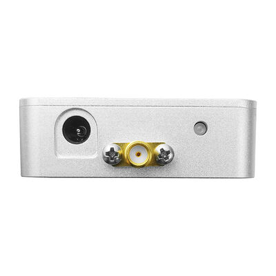
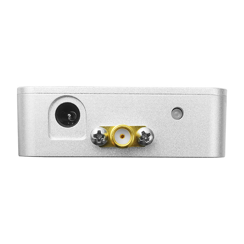
■ MMCX-KEF input connector 50 Ω
■ MMCX-KEF input connector 50 Ω
■ Power supply voltage 12~31V option
■ Temperature:-40~+70℃
■ RFout +RFinput+enable wire
■ ingle-carrier modulation technology
Applications
■ Wireless communication field
■ Drone FPV enthusiasts
TXSZS520010 Data sheet
| Functional Unit |
parameter |
MINI |
Typical Value |
Max |
Unit |
Remark |
|
General
Requirements
|
Duplex mode |
TDD |
|
|
| Operating frequency |
5100 |
|
5800 |
MHz |
Customized |
| Supply voltage |
12 |
24 |
31 |
V |
|
| Operating temperature |
-40 |
|
70 |
℃ |
|
|
Transmitter way
|
Transmitter gain |
18±1 |
|
22±1 |
dB |
Customized |
| Maximum output power(P1dB) |
|
47 |
|
dBm |
|
| Linear output power |
|
31 |
|
dBm |
EVM<5% |
|
EVM@Pout=38dBm
|
|
-30
|
|
dB
|
|
| In-band fluctuation |
|
0.3 |
0.3 |
dB |
|
| Working current |
|
0.3 |
0.25 |
A |
@Pout=40dBm, VCC=24V |
| Switching delay |
|
|
1 |
us |
|
| Second Harmonic |
-65 |
|
-50 |
dBc |
|
| Second Harmonic |
|
|
-60 |
dBc |
|
|
Receiving way
|
Receive gain |
14 |
|
15 |
dB |
Customized |
| Noise Figure |
|
2.5 |
3 |
dB |
|
| Working current |
|
11 |
|
mA |
|
| In-band fluctuation |
|
|
0.2 |
dB |
|
TXSZS520010 Storage environment requirements
a) Temperature: -40~+70℃;
b) Operating relative humidity: 5%~95%, non-condensing;
c) Atmospheric pressure: (70~106) kPa;
d) Humidity and heat: Can operate in high-temperature and high-relative-humidity environments with temperatures not lower than 40℃ and relative humidity not lower than 95%;
e) Storage temperature: -40~+125℃;
f) Storage humidity: 5%~98%, non-condensing.
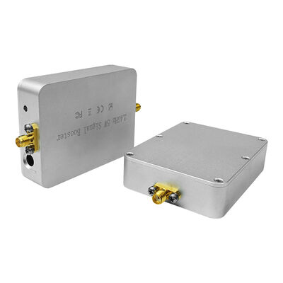
TXSZS520010 detail picture

TXSZS520010 sell service
User Instruction: we can offer online details photo illustration and video;local instruction is also available but with extra costOnline technical support:our professional engineers will assist customers with technical problems
After sales service:
our company will perform the agreed responsibility and duty during the warranty period
Fast reply of Customer feedback and questions
All product enjoy 1 year warranty and Life time maintenance service
FAQ
How can i get the price ?
We usually quote within 24 hours after we get your inquiry. If you are very urgent to get the price, please tell us in your
email so that we will regard you inquiry priority.
Are you manufacture ?
yes ,we are the real factory located in ShenZhen China ,we support all the products customized .And also we support visit factory by yourself .
How to guarantee the goods quality ?
We have advance technology and testing equipment ,before shipment we will 100% test .
Ratings & Review

 Your message must be between 20-3,000 characters!


Overall Rating
Rating Snapshot
The following is the distribution of all ratingsAll Reviews