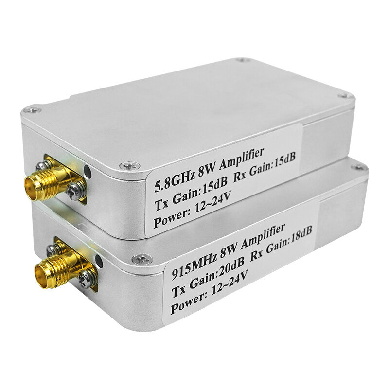
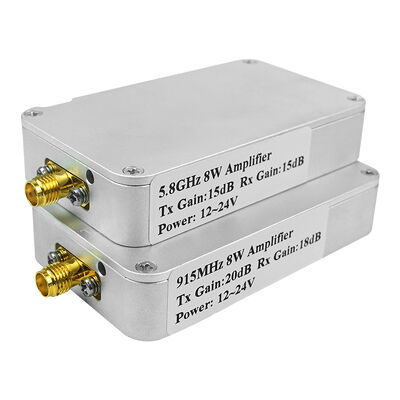
RX with TX WIFI 2.4ghz 10W 12V dual band fpv drone signal extender rf power amplifier
This product adopts the leading single carrier modulation technology, has a very long air transmission distance and strong anti-interference ability, and matches with frequency extension technologies such as direct sequence (DSSS) and orthogonal frequency division multiplexing (OFDM), which greatly expands the wireless RF communication distance while ensuring that the transmission rate of wireless devices remains unchanged. The product has the advantages of small size, high efficiency, good linearity, stability and reliability.
Features
■ 2300-2400 Frequency Range
■ 12-31V voltage option
■ Working current around 1A
■ Operating Humidity Up to 95% humidity
■ Input Trigger Power Min:10dBm Max:26dBm
■ EVM:3%@33dBm 802.11g 54Mbps OFDM 64QAM BW 20MHz
■ Receiving Gain16dB±1
■ Transmission Gain 18dB±1
■ TX/RX Switch Time Delay<1 us
Data sheet
| Functional Unit |
parameter |
MINI |
Typical Value |
Max |
Unit |
Remark |
|
General
Requirements
|
Duplex mode |
TDD |
|
|
| Operating frequency |
2300 |
|
2400 |
MHz |
Customized |
| Supply voltage |
12 |
24 |
31 |
V |
|
| Operating temperature |
-40 |
|
70 |
℃ |
|
|
Transmitter way
|
Transmitter gain |
10 |
20 |
40 |
dB |
Customized |
| Maximum output power(P1dB) |
|
47 |
|
dBm |
|
| Linear output power |
|
40 |
|
dBm |
EVM<3% |
|
EVM@Pout=38dBm
|
|
-30
|
|
dB
|
802.11g 54Mbps
OFDM 64QAM
BW 20MHz
|
| In-band fluctuation |
|
0.4 |
0.5 |
dB |
|
| Working current |
|
1 |
1.2 |
A |
@Pout=40dBm, VCC=24V |
| Switching delay |
|
|
1 |
us |
|
| Second Harmonic |
-65 |
|
-50 |
dBc |
|
| Second Harmonic |
|
|
-60 |
dBc |
|
|
Receiving way
|
Receive gain |
15 |
17 |
25 |
dB |
Customized |
| Noise Figure |
|
2.5 |
3 |
dB |
|
| Working current |
|
10 |
|
mA |
|
| In-band fluctuation |
|
|
0.3 |
dB |
|
Working and storage environment requirements
a) Temperature: -40~+70℃;
b) Working relative humidity: 5%~95%, no condensation;
c) Atmospheric pressure: (70~106) kPa;
d) Humidity: Able to work in a high temperature and high relative humidity environment with a temperature not lower than 40℃ and a relative humidity not lower than 95%;
e) Storage temperature: -40~+125℃;
f) Storage humidity: 5%~98%, no condensation.
Precautions for use
If the output power is greater than 5W and above, it is recommended to strengthen the heat dissipation
treatment,such as adding a heat sink or adding a fan.
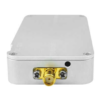
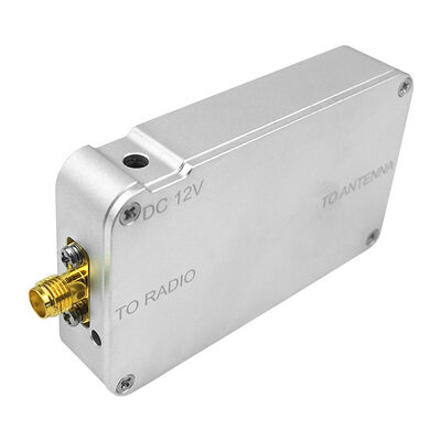
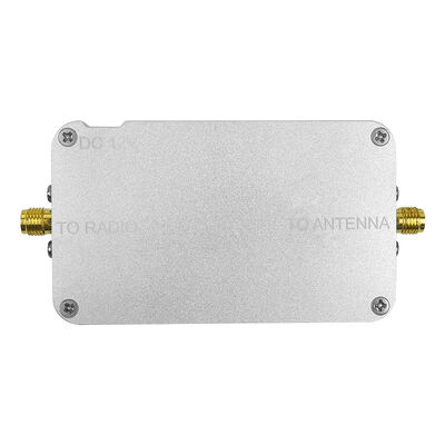
When connecting, you must first screw on the antenna, then connect the front-end source device, and finally supply powe
Please use the correct voltage matching the power amplifier .
After sales service:
our company will perform the agreed responsibility and duty during the warranty period
Fast reply of Customer feedback and questions
All product enjoy 1 year warranty and Life time maintenance service
FAQ
How can i get the price ?
We usually quote within 24 hours after we get your inquiry. If you are very urgent to get the price, please tell us in your
email so that we will regard you inquiry priority.
Are you manufacture ?
yes ,we are the real factory located in ShenZhen China ,we support all the products customized .And also we support visit factory by yourself .
How to guarantee the goods quality ?
We have advance technology and testing equipment ,before shipment we will 100% test .
Ratings & Review

 Your message must be between 20-3,000 characters!


Overall Rating
Rating Snapshot
The following is the distribution of all ratingsAll Reviews